- 您现在的位置:买卖IC网 > Sheet目录378 > 2V7002LT1G (ON Semiconductor)MOSFET N-CH 60V 115MA SOT-23-3
�� �
�
�2N7002L,� 2V7002L�
�Small� Signal� MOSFET�
�60� V,� 115� mA,� N� ?� Channel� SOT� ?� 23�
�Features�
�?� 2V� Prefix� for� Automotive� and� Other� Applications� Requiring� Unique�
�Site� and� Control� Change� Requirements;� AEC� ?� Q101� Qualified� and�
�http://onsemi.com�
�PPAP� Capable� (2V7002L)�
�?� These� Devices� are� Pb� ?� Free,� Halogen� Free/BFR� Free� and� are� RoHS�
�Compliant�
�MAXIMUM� RATINGS�
�V� (BR)DSS�
�60� V�
�R� DS(on)� MAX�
�7.5� W� @� 10� V,�
�500� mA�
�I� D� MAX�
�115� mA�
�Rating�
�Drain� ?� Source� Voltage�
�Drain� ?� Gate� Voltage� (R� GS� =� 1.0� M� W� )�
�Drain� Current�
�?� Continuous� T� C� =� 25� °� C� (Note� 1)�
�?� Continuous� T� C� =� 100� °� C� (Note� 1)�
�?� Pulsed� (Note� 2)�
�Symbol�
�V� DSS�
�V� DGR�
�I� D�
�I� D�
�I� DM�
�Value�
�60�
�60�
�±� 115�
�±� 75�
�±� 800�
�Unit�
�Vdc�
�Vdc�
�mAdc�
�1�
�N� ?� Channel�
�3�
�Gate� ?� Source� Voltage�
�?� Continuous�
�?� Non� ?� repetitive� (t� p� ≤� 50� m� s)�
�THERMAL� CHARACTERISTICS�
�Characteristic�
�Total� Device� Dissipation� FR� ?� 5� Board�
�(Note� 3)� T� A� =� 25� °� C�
�Derate� above� 25� °� C�
�Thermal� Resistance,� Junction� ?� to� ?� Ambient�
�V� GS�
�V� GSM�
�Symbol�
�P� D�
�R� q� JA�
�±� 20�
�±� 40�
�Max�
�225�
�1.8�
�556�
�Vdc�
�Vpk�
�Unit�
�mW�
�mW/� °� C�
�°� C/W�
�1�
�3�
�2�
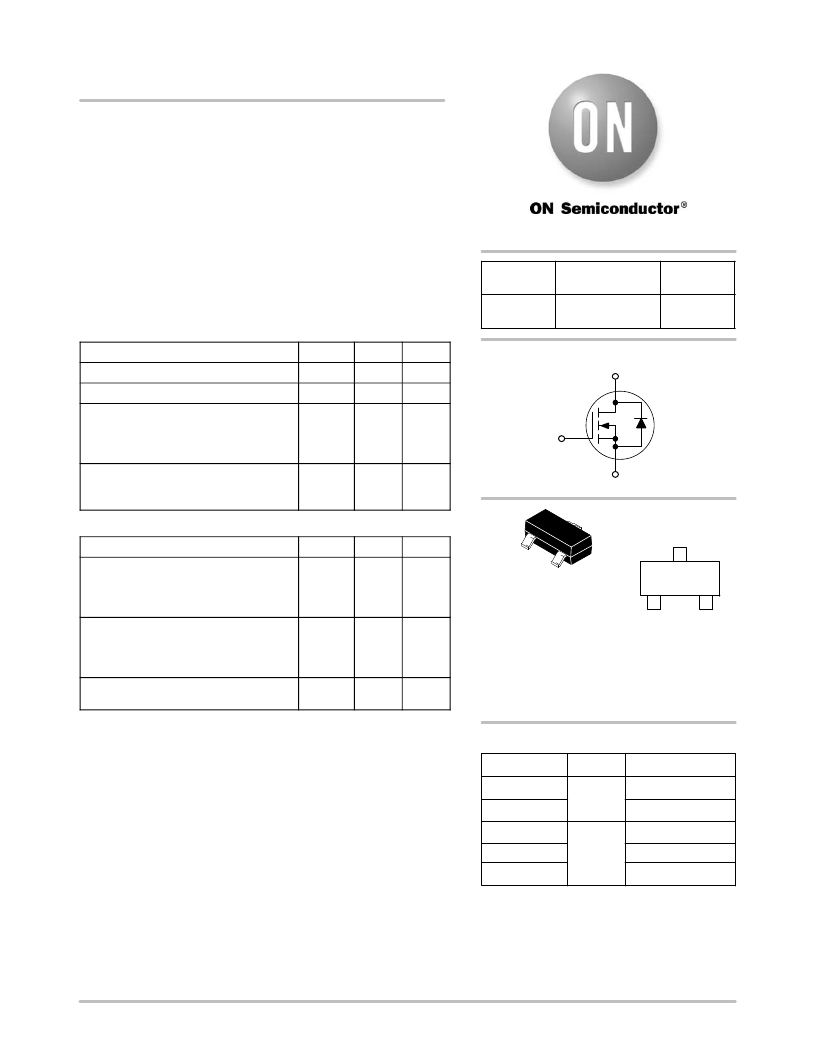
�SOT� ?� 23�
�CASE� 318�
�2�
�1�
�MARKING�
�DIAGRAM�
�702� M� G�
�G�
�(Note� 4)� Alumina� Substrate,� T� A� =� 25� °� C�
�Derate� above� 25� °� C�
�Thermal� Resistance,� Junction� ?� to� ?� Ambient�
�2N7002LT3G�
�10,000� Tape� &� Reel�
�Total� Device� Dissipation� P� D�
�300� mW�
�2.4� mW/� °� C�
�R� q� JA� 417� °� C/W�
�Junction� and� Storage� Temperature� T� J� ,� T� stg� ?� 55� to� °� C�
�+150�
�Stresses� exceeding� Maximum� Ratings� may� damage� the� device.� Maximum�
�Ratings� are� stress� ratings� only.� Functional� operation� above� the� Recommended�
�Operating� Conditions� is� not� implied.� Extended� exposure� to� stresses� above� the�
�Recommended� Operating� Conditions� may� affect� device� reliability.�
�1.� The� Power� Dissipation� of� the� package� may� result� in� a� lower� continuous� drain�
�current.�
�2.� Pulse� Test:� Pulse� Width� ≤� 300� m� s,� Duty� Cycle� ≤� 2.0%.�
�3.� FR� ?� 5� =� 1.0� x� 0.75� x� 0.062� in.�
�4.� Alumina� =� 0.4� x� 0.3� x� 0.025� in� 99.5%� alumina.�
�STYLE� 21�
�702� =� Device� Code�
�M� =� Date� Code*�
�G� =� Pb� ?� Free� Package�
�(Note:� Microdot� may� be� in� either� location)�
�*Date� Code� orientation� and/or� position� may�
�vary� depending� upon� manufacturing� location.�
�ORDERING� INFORMATION�
�Device� Package� Shipping� ?�
�2N7002LT1G� SOT� ?� 23� 3000� Tape� &� Reel�
�(Pb� ?� Free)�
�2V7002LT1G�
�3000� Tape� &� Reel�
�2V7002LT3G�
�2N7002LT1H*�
�SOT� ?� 23�
�(Pb� ?� Free)�
�10,000� Tape� &� Reel�
�3000� Tape� &� Reel�
�?For� information� on� tape� and� reel� specifications,�
�including� part� orientation� and� tape� sizes,� please�
�refer� to� our� Tape� and� Reel� Packaging� Specifications�
�Brochure,� BRD8011/D.�
�*Not� for� new� design.�
�?� Semiconductor� Components� Industries,� LLC,� 2013�
�April,� 2013� ?� Rev.� 7�
�1�
�Publication� Order� Number:�
�2N7002L/D�
�发布紧急采购,3分钟左右您将得到回复。
相关PDF资料
2V7002WT1G
MOSFET N-CH 60V 310MA SC70-3
30 PSI-G-4V
SENSOR 30PSIG 4V DUAL
3003308
SHIELDING TAPE COPPER 8MMX33M
3003310
SHIELDING TAPE COPPER 10MMX33M
3003320
SHIELDING TAPE COPPER 20MMX33M
3003325
SHIELDING TAPE COPPER 25MMX33M
3003350
SHIELDING TAPE COPPER 50MMX33M
3013308
SHIELDING TAPE ALUM 8MMX33M
相关代理商/技术参数
2V7002LT3G
功能描述:MOSFET NFET 60V 115MA 7.5O
RoHS:否 制造商:STMicroelectronics 晶体管极性:N-Channel 汲极/源极击穿电压:650 V 闸/源击穿电压:25 V 漏极连续电流:130 A 电阻汲极/源极 RDS(导通):0.014 Ohms 配置:Single 最大工作温度: 安装风格:Through Hole 封装 / 箱体:Max247 封装:Tube
2V7002W
制造商:ONSEMI 制造商全称:ON Semiconductor 功能描述:Small Signal MOSFET 60 V, 340 mA, Single, N.Channel, SC.70
2V7002WT1G
功能描述:MOSFET NFET 60V 115MA 7OHM RoHS:否 制造商:STMicroelectronics 晶体管极性:N-Channel 汲极/源极击穿电压:650 V 闸/源击穿电压:25 V 漏极连续电流:130 A 电阻汲极/源极 RDS(导通):0.014 Ohms 配置:Single 最大工作温度: 安装风格:Through Hole 封装 / 箱体:Max247 封装:Tube
2V7BC
制造商:SEMTECH_ELEC 制造商全称:SEMTECH ELECTRONICS LTD. 功能描述:Silicon Epitaxial Planar Zener Diodes
2V7BCA
制造商:SEMTECH_ELEC 制造商全称:SEMTECH ELECTRONICS LTD. 功能描述:Silicon Epitaxial Planar Zener Diodes
2V7BCB
制造商:SEMTECH_ELEC 制造商全称:SEMTECH ELECTRONICS LTD. 功能描述:Silicon Epitaxial Planar Zener Diodes
2V7BS
制造商:SEMTECH_ELEC 制造商全称:SEMTECH ELECTRONICS LTD. 功能描述:SILICON PLANAR ZENER DIODES
2V7BSA
制造商:SEMTECH_ELEC 制造商全称:SEMTECH ELECTRONICS LTD. 功能描述:SILICON PLANAR ZENER DIODES